The die is not the whole product
May 24, 2026The word “chip” makes the product sound smaller than it is.
A die is the piece of silicon where the circuits live. It is easy to point at that square and call it the chip. But that square is only one layer of the product. An advanced AI accelerator also includes memory beside the die and tiny bridges between pieces. It includes the base underneath, solder, the circuit board, the cold plate, and the factory recipe that has to build the same stack thousands of times.
At this size, the package is not a wrapper. It carries memory traffic, power, heat, mechanical stress, and manufacturing risk.
What the package has to do
A chip starts as part of a round silicon wafer. The factory cuts the wafer into small rectangles called dies. Then the die goes into a package, the physical home that gives it power, cooling, and links to the rest of the machine.
That flow breaks down for AI accelerators. An AI accelerator is hardware built to run neural-network math quickly. A large model wants lots of compute, which means lots of circuits doing math. It also wants nearby memory, because the math is useless if the numbers arrive too slowly.
There is a manufacturing limit here called the reticle limit. A reticle is the largest rectangle a chipmaking machine can print at one time. If an AI processor wants to be bigger than that, the designer has to join pieces together after they are made.
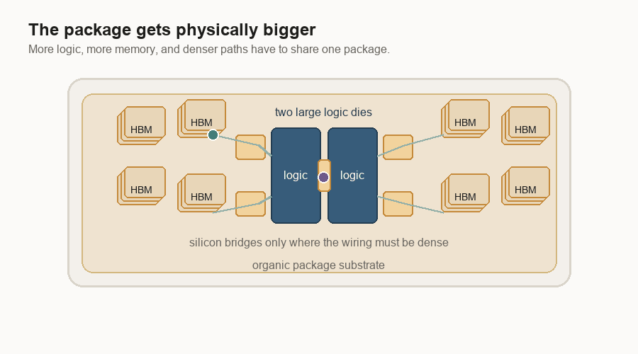
Advanced packaging joins the pieces. Put two logic dies on the same package. A logic die is a piece of silicon that does the main computation. Put HBM next to them. HBM means high-bandwidth memory, a stack of memory chips built to feed data quickly.
Then use silicon bridges or a silicon interposer to connect everything. A bridge is a small piece of silicon used as a short, dense wiring path. An interposer is the larger version: a silicon layer that sits under chips and carries many wires between them.
This can make several pieces act like one bigger processor. But now the package is doing much more than holding a chip. It is carrying the most important traffic in the system.
The clean diagram hides the assembly problem. The package is a stack of different materials. Some parts are silicon. Some sit on an organic substrate, which is the board-like base under the chips. Some parts are solder. Some are copper-heavy board or cooling metal. The links between them are tiny, but the whole package is getting physically larger.
The bridge has to land
Placement is unforgiving.
A bridge only works if it lands under the right metal contact points. Those contact points are often called bumps or pads. I think of them as the chip’s tiny plugs and sockets. If the bridge is shifted too far, the plugs no longer meet the sockets.
At human scale, the drawing looks forgiving. Slide the bridge a little and it still seems to sit under both chips. At manufacturing scale, a small shift can break the connection.
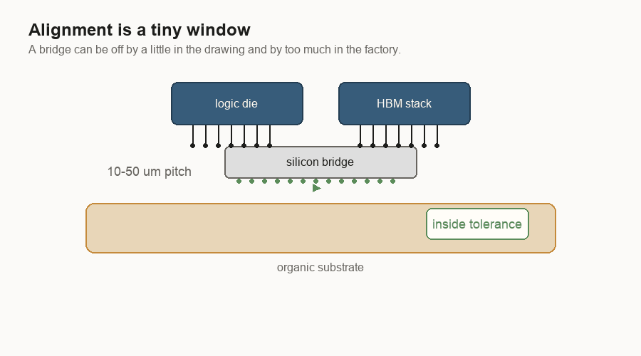
That is why prototypes can mislead. A lab can make a small number of packages work. A production line has to make many of them work, with the same alignment window, across normal variation in tools, materials, and temperature.
One working package proves less than a process that keeps building it.
Heat moves the target
The package also moves. When it heats up, each material grows by a different amount.
Engineers call this CTE, or coefficient of thermal expansion. In plain English: how much a material stretches when it gets hotter.
The rough numbers are easy to remember. Silicon grows about 2.6 parts per million for each degree Celsius. Some organic package materials grow around 10. Copper-heavy circuit boards or cold plates can grow around 17. Those sound like tiny numbers. But the package is large, the contacts are tiny, and the temperature keeps changing.
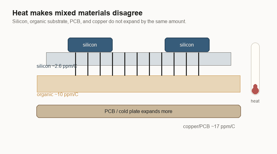
If everything in the package were silicon, the pieces would move more together. Once the package mixes silicon bridges with organic substrate and board-level materials, the pieces try to move different distances.
That creates bowing. The package can curve. Solder joints can be pulled. Layers can delaminate. A bridge can be aligned at the beginning and still live in a structure that wants to move around it.
A chip can work as a circuit and still struggle as a product. It has to survive heat, assembly, shipping, and repeated use.
Volume is its own problem
A working sample can still be far from a shippable product. The gap is volume manufacturing: making the same thing in large numbers.
In software, a prototype can be crude and still show the right idea. In hardware, the prototype can hide the yield problem. One package can pass. Ten can pass. Then the factory tries to build thousands, and the small variation that was invisible before becomes the whole problem.
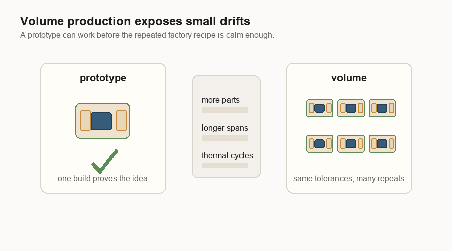
This is why “it works” is not the same as “it ships.” The production version has to work across small changes in tools, material batches, temperature cycles, handling, and rework. It also needs good yield. Yield is the share of parts that come out usable.
Every generation asks the package to do more: more memory speed, more memory capacity, more logic, more power, more cooling, and more communication between pieces. The package is not a wrapper anymore. It is part of how the computer gets faster.
The wafer-scale bet
A wafer-scale design makes the opposite bet. Instead of cutting a wafer into dies and then putting selected dies back together in a package, it keeps the wafer as one large processor.
At first, that looks risky. A normal wafer has defects. If one defect can ruin the whole machine, the idea falls apart.
The design uses many small cores. A core is a small compute block. If one core is bad, the system can route around it. The software above the chip can still see one usable machine.
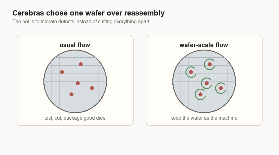
The tolerance is different. In a GPU, a large damaged block can cost a lot because the block is a big piece of the product. In a wafer-scale machine, a small bad core can become a local detour.
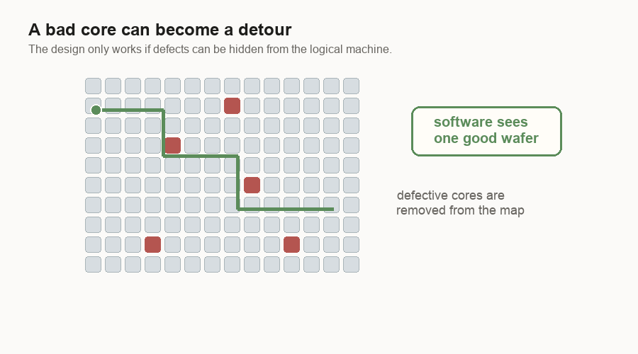
For me, that changes the yield question. The question is not “can the wafer be perfect?” It is “how much imperfection can the design hide?”
This is a software idea hiding in hardware. The wafer does not have to be perfect if the machine can hide small bad spots from the user.
Memory wants to be close
The wafer-scale design also changes where memory lives.
AI chips spend much of their energy moving data. Logic means the circuits that do the math. Memory stores the numbers the math needs. If logic is far from memory, the system pays in latency, energy, and bandwidth pressure. Latency is waiting time. Bandwidth is how much data can move at once.
On a single wafer, the fast working memory is not one far-away block. It is spread through the wafer as local SRAM beside groups of cores. SRAM is fast memory built into the silicon. It is smaller than the big HBM, or high-bandwidth memory, stacks beside many GPUs, but it is much closer to the math.
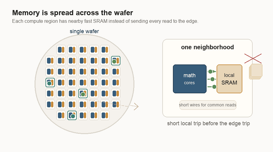
That does not mean every number stays local forever. It means the common reads and writes can often take a short path, and the software can try to keep work near the data it uses.
The math is not enough. Where the numbers live matters.
Short wires help with the memory bandwidth wall. They are cheaper to use than long wires. That wall is what happens when the math is ready but the data cannot arrive fast enough. The more technical word is capacitance: a wire’s tendency to hold electrical charge. More capacitance takes more energy to switch. Shorter wires usually mean less capacitance, which means less energy to move a signal. Distributed memory means a core does not always need a long trip to a central memory edge.
Memory placement is physical, not a cache diagram. The location of the memory on the package changes the cost of using it.
Native wires beat placed bridges
The same logic shows up at reticle boundaries. A reticle boundary is the edge between two printed regions on the wafer. If the regions are still part of the same wafer, their wiring can be made by the same lithography process that made the rest of the chip wiring. Lithography is the printing process used to draw circuits onto silicon.
If two dies were cut apart and later put back together, the connection between them needs a bridge, interposer, or some other package-level structure.
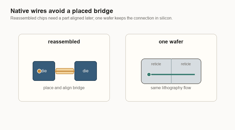
A bridge is not just a wire. It is a part that has to be placed, aligned, bonded, cooled, and trusted through heat cycles. A native wafer connection is still difficult, but it avoids one whole class of “put the pieces back together” problems.
Wafer-scale is not a universal answer. Each design chooses its hard problem. A wafer-scale machine has to hide local defects. A multi-die GPU has to put separate high-speed pieces back together in one package.
The recipe gets simpler in one dimension
A wafer-scale processor is not simple. It is a huge bet on manufacturing, routing, cooling, power, and fault tolerance. Fault tolerance means the system keeps working when small parts fail.
But at the package level, the comparison is real. A multi-die package made from separate pieces has more sensitive ingredients: logic dies, memory stacks, bridges or interposers, organic substrate, solder joints, PCB, thermal interface material, and cold plate. PCB means printed circuit board. Thermal interface material is the soft layer that helps heat move from the chip into the cooler. Each interface has to line up and survive.
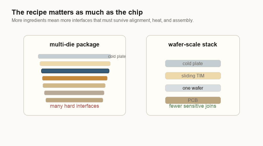
That is the trade I see now:
| Approach | What it tries to avoid | What it must solve instead |
|---|---|---|
| Multi-die package | Huge one-piece dies and wafer-scale defect exposure | Bridge/interposer alignment, materials expanding differently, assembly yield |
| Wafer-scale engine | Cutting and reassembling many dense pieces | Hiding bad spots, wafer-level routing, large-surface power and cooling |
Both are hard. The work moves to different places.
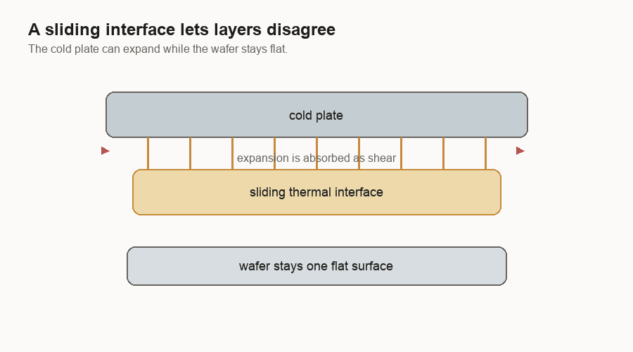
Cooling is also mechanical design
Cooling and power get their own mechanical problems.
A wafer-scale system still needs a cold plate. A cold plate is a metal cooling block that carries heat away. The system still needs a PCB too. It has to move heat out and power in. The difference is that a single wafer can be flat. A flat wafer can meet a flat cold plate through a more even thermal interface.
In a reconstructed package, different dies can have slightly different heights, different heat levels, and different expansion behavior. The thermal interface has to flex up and down, while the electrical side has its own connections that may not want to move.
Electrical connections have the same problem. Near the center of a wafer, a connection can be more direct. Toward the edges, the PCB and wafer want to move by different amounts as temperature changes. A flexible connector can let the two large surfaces expand differently while maintaining contact.
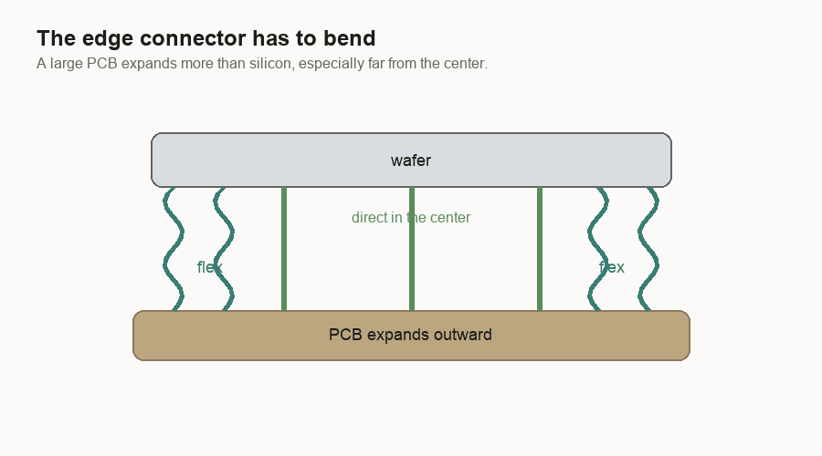
The system is not pretending materials will stop expanding. It gives the expansion somewhere to go.
At this scale, the package is not the box around the computer. It is part of the computer.
Source: Cerebras.